
Solid state technologies break into medical imaging
Solid state imaging technologies have revolutionised medical imaging equipment from X-ray machines to ultrasonic scanners, writes Sally Ward-Foxton.
A recent report by industry analysts Yole Développement reveals that solid state imaging ICs are now able to offer disruptive technologies at competitive prices to the medical imaging market. These include well known imaging technologies such as Charge Coupled Devices (CCD) and CMOS imaging sensors, alongside a whole host of new specialised technologies which operate solely in their specific medical niches. The same report places the market for equipment using these technologies at $35bn in 2016 with a 5.5% CAGR until 2022 (see Figure 1).
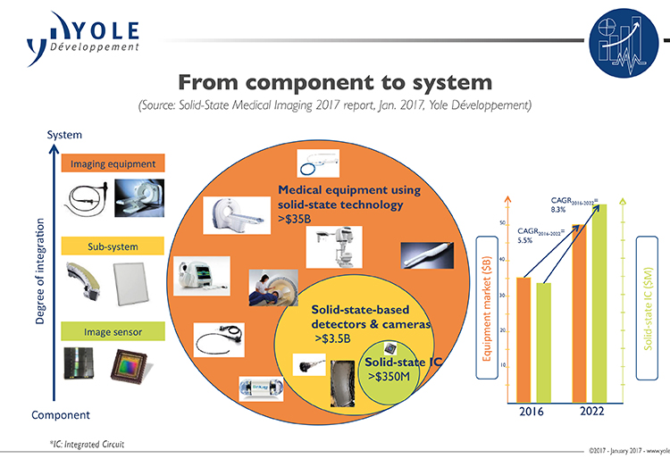
Above: Figure 1. The size of the medical imaging equipment market between 2016 and 2022 (source: Yole)
“The technologies and related use cases are constantly evolving, providing space for innovators to differentiate themselves,” said Jérôme Mouly, Technology and Market Analyst at Yole. “Numerous new solid state innovations are ready to enter the market.”
Since X-rays were discovered in 1895, medical imaging has become an extremely high tech field (see Figure 2), including Magnetic Resonance Imaging (MRI), Computed Tomography (CT) scanning and endoscopy. Today’s solid state digital imaging technology, including CCD and CMOS image sensors, enables tiny endoscopes, camera pills and other futuristic devices.
CCD and CMOS
CCD and CMOS image sensors are both well known and well used, not just in medical imaging, but across practically every imaging field.
CCDs are used to produce high quality images in everything from X-ray machines to camera pills (for non-visible light such as X-rays, there is a scintillation layer which converts X-rays to visible light, which is then typically directed into the sensor via a mirror). These sensors have a photoactive area of silicon above each pixel onto which the image to be captured is projected through a lens. An electric charge proportional to the light intensity at that pixel location is accumulated in capacitor structures at each pixel in the array. Each pixel in the array shifts its charge to its neighbour sequentially until the charges reach a charge amplifier at the end of each row. The amplifier converts the charge from each pixel in the row into a sequence of voltages which can be sampled, digitised and stored.
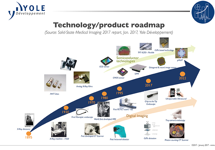
Figure 2. A technology roadmap for the medical imaging sector from the discovery of X-rays to today (source: Yole).
CMOS Image Sensors (sometimes called CIS) use an array of photodiodes with an amplifier attached to every pixel, allowing much faster image processing than a CCD. Scalability issues for large CCD panels are also solved in this setup. The amplifiers take up space between the pixels’ active area, but this is usually solved with an array of microlenses which focusses the light falling on each pixel onto the active area.
CMOS image sensors are widely used today in everything from smartphone cameras to DSLRs, as they are generally cheaper than CCD sensors and consume less power. They are also very quick and offer high resolution images. CCD has become practically extinct in the consumer market as a result. However, for specialist fields like medical imaging, CCDs are still preferred in some applications such as ophthalmology cameras as they can capture better images in low light conditions and introduce less noise for long exposure times. Indeed, the medical imaging CCD market is predicted to remain stable over the coming years (see Figure 3).
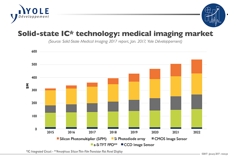
Figure 3. Predicted market for different medical imaging technologies up to 2022 (source: Yole)
a-Si FPD devices
Medical amorphous Silicon Flat Panel Detectors (a-Si FPD) use a pixel array directly behind the scintillation layer. The pixels comprise a photodetector and a TFT (Thin Film Transistor) in a similar configuration to an LCD panel. The signals from the photodiodes are amplified and processed by other electronics behind the display or at the edges. Since flat panel detectors’ electronics are directly exposed to the X-ray source (unlike in CCDs), they need to be radiation hardened to avoid being damaged by X-rays. Some damage is still inevitable meaning the panels often come with relatively high maintenance costs compared to other technologies.
This technology isn’t new, and though the technology is relatively slow with low resolution, its simplicity and ability to be built in large panels makes it suitable for certain applications. a-Si FPDs can be built in compact packaging, like the Varian Imaging PaxScan 3024M, intended for mammography, which measures 30x24cm - small enough for mobile screening applications.
Si PM
Silicon Photo Multipliers (SiPMs) are a specialist type of imaging sensor used in PET (Positron Emission Topology) and SPECT (Single Photon Emission Computed Tomography) applications. These applications use a radioactive tracer which is introduced into the patient either by inhalation, swallowing or injection. PET and SPECT scanners detect very tiny amounts of radiation emitted by the tracer material as it travels in the body. This technique is now a standard part of cancer treatment so the demand for SiPMs is increasing (see Figure 3).
Traditionally, these scanners used glass vacuum tubes called photomultiplier tubes, which had been in use since the 1950s. SiPMs replace these tubes with a silicon based sensor which is not magnetic – meaning SiPM detectors can be combined with MRI machines for multi-modal imaging. SiPMs can proide high gain, operate on low voltage and respond quicker than tube based sensors. They are also compact and rugged.
SiPM uses avalanche photodiodes which can detect photons incident on their pixels. These photodiodes operate in ‘Geiger mode’ in which a single incident photon is enough to trigger an avalanche current. Time of flight measurement is also possible.
cMUT
One of the newest technologies emerging in this sector is capacitive Micromachined Ultrasonic Transducers (cMUT). cMUT devices are used in sonography (ultrasound imaging) where they offer higher resolution, higher speed and real-time 3D imaging.
The incumbent technology, which is based on bulk piezoelectric ceramic materials, is reaching its limit in terms of miniaturisation and resolution. Piezoelectric transducers are often used in a row to produce a 2D image. cMUT transducers are MEMS structures built on a Si or CMOS substrate.
The MEMS portion is a thin membrane suspended over a sealed cavity. The membrane and the cavity walls act as electrodes; when an AC voltage with the right DC bias is applied, the membrane vibrates at the right frequency to produce ultrasound signals. If reflected ultrasound waves hit the membrane, it vibrates to produce an AC signal. Because these devices are built as integrated circuits, high frequency, high resolution 3D transducers can be made easily and more cost effectively. The frequency is increased by reducing the size of the cavity, which is relatively easy to do, and the pixels’ small size means a broad bandwidth can be achieved.
While cMUT transducers are relatively new to the market, there are several commercial products available today.
Product Spotlight
APV1111GVY
Panasonic

Panasonic PhotoMOS® Photovoltaic MOSFET High-Power Drivers
| SKU: | |
|---|---|
| Stock: | 3490 |
| Cost: | $3.95 |
